- 您现在的位置:买卖IC网 > Sheet目录505 > RXD-433-KH2 (Linx Technologies Inc)RECEIVER/DECODER 433MHZ KH2 SER
�� �
�
�ENCODER� OPERATION�
�POWER� SUPPLY� REQUIREMENTS�
�The� KH2� Series� transmitter� internally� utilizes�
�the� HT640� encoder� from� Holtek.� The�
�Power� On�
�The� module� does� not� have� an� internal� voltage�
�regulator;� therefore� it� requires� a� clean,� well-regulated�
�Vcc� TO�
�MODULE�
�encoder� begins� a� three-word� transmission�
�cycle� when� the� Transmission� Enable� line�
�(TE)� is� pulled� high.� This� cycle� will� repeat�
�itself� for� as� long� as� the� TE� line� is� held� high.�
�Standby� Mode�
�power� source.� While� it� is� preferable� to� power� the� unit�
�from� a� battery,� it� can� also� be� operated� from� a� power�
�supply� as� long� as� noise� is� less� than� 20mV.� Power�
�supply� noise� can� affect� the� transmitter� modulation;�
�Vcc� IN�
�10� Ω�
�10� μ� F�
�Once� TE� falls� low,� the� encoder� output�
�therefore,� providing� a� clean� power� supply� for� the�
�A� 10� Ω� resistor� in� series� with� the� supply� followed� by� a�
�completes� its� final� cycle� and� then� stops� as�
�shown� in� the� Encoder� /� Decoder� Timing�
�diagram.� When� a� transmission� enable� signal�
�is� applied,� the� encoder� scans� and� transmits�
�the� status� of� the� 10� bits� of� the� address� code�
�and� the� 8� bits� of� the� data� serially� in� the� order�
�A0� to� A9,� D0� to� D7.�
�The� status� of� each� address� /� data� pin� can� be�
�individually� preset� to� logic� high,� low,� or�
�floating.� The� floating� state� on� the� data� input�
�is� interpreted� as� logic� low� by� the� decoders�
�since� the� decoder� output� only� has� two�
�states.� The� address� pins� are� usually� set� to�
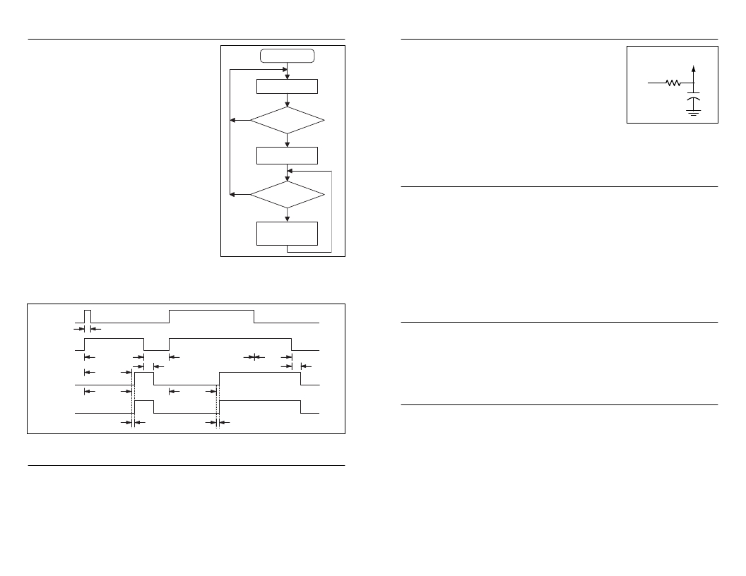
�No�
�Transmission�
�Enabled?�
�Yes�
�3� Data� Words�
�Transmitted�
�Transmission�
�Still� Enabled?�
�3� Data� Words�
�Transmitted�
�Continuously�
�module� should� be� a� high� priority� during� design.�
�Figure� 10:� Supply� Filter�
�10μF� tantalum� capacitor� from� V� CC� to� ground� will� help� in� cases� where� the� quality�
�of� supply� power� is� poor.� These� values� may� need� to� be� adjusted� depending� on�
�the� noise� present� on� the� supply� line.�
�DATA� INPUTS�
�When� the� Transmit� Enable� (TE)� line� goes� high,� the� states� of� the� eight� data� input�
�lines� are� recorded� and� encoded� for� transmission.� The� data� lines� are� tri-state,�
�which� means� that� they� can� be� high,� low,� or� floating,� though� the� decoder� will�
�interpret� the� floating� state� as� a� low.� This� feature� means� that� the� data� lines� do� not�
�require� pull-up� or� pull-down� resistors.� The� states� of� the� data� lines� can� be� set� by�
�switches,� jumpers,� microcontrollers,� or� hardwired� on� the� PCB.�
�switches� or� PCB� wiring,� while� the� data� is�
�transmit� particular� security� codes� by� DIP�
�Figure� 8:� Encoder� Flowchart�
�selected� using� push� buttons� or� electronic�
�switches.� The� floating� state� allows� the� KH2� transmitter� to� be� used� without� pull-�
�up� or� pull-down� resistors� on� the� data� and� address� input� lines.�
�Encoder�
�Transmit�
�The� encoder� will� send� the� states� of� the� address� and� data� lines� three� times.� If� the�
�TE� line� is� still� high,� it� will� begin� the� cycle� again.� This� means� that� the� states� of� the�
�data� lines� are� refreshed� with� each� cycle,� so� the� data� lines� can� be� changed�
�without� having� to� pull� TE� low.� There� can� be� up� to� a� 150mS� lag� in� response� as�
�the� transmitter� finishes� one� cycle� then� refreshes� and� starts� over.�
�ENABLING� TRANSMISSION�
�Enable�
�Encoder�
�<� 1� Word�
�The� module’s� Transmit� Enable� (TE)� line� controls� transmission� status.� When�
�taken� high,� the� module� initiates� transmission,� which� continues� until� the� line� is�
�2�
�Data� Out�
�Decoder� VT�
�3� Words�
�2� Words�
�14�
�Transmitted� Continuously�
�Clocks�
�3� Words�
�2�
�14�
�Clocks�
�pulled� low� or� power� to� the� module� is� removed.� In� some� cases� this� line� will� be�
�wired� permanently� to� V� CC� and� transmission� controlled� by� switching� V� CC� to� the�
�module.� This� is� particularly� useful� in� applications� where� the� module� powers� up�
�and� sends� a� transmission� only� when� a� button� is� pressed� on� the� remote.�
�Decoder�
�Data� Out�
�Check�
�Check�
�1/2� Clock� Time�
�1/2� Clock� Time�
�USING� LADJ�
�The� LADJ� line� allows� the� transmitter’s� output� power� to� be� easily� adjusted� for�
�range� control,� lower� power� consumption,� or� to� meet� legal� requirements.� This� is�
�Figure� 9:� Encoder� /� Decoder� Timing� Diagram�
�SETTING� THE� TRANSMITTER� ADDRESS�
�The� module� provides� ten� tri-state� address� lines.� This� allows� for� the� formation� of�
�up� to� 59,049� (3� 10� )� unique� transmitter-receiver� relationships.� Tri-state� means� that�
�the� address� lines� have� three� distinct� states:� high,� low,� or� floating.� These� pins�
�may� be� hardwired� or� configured� via� a� microprocessor,� DIP� switch,� or� jumpers.�
�The� receiver’s� address� line� states� must� match� the� transmitter’s� exactly� for� a�
�transmission� to� be� recognized.� If� the� transmitted� address� does� not� match� the�
�receiver’s� local� address,� then� the� receiver� will� take� no� action.�
�Page� 6�
�done� by� placing� a� resistor� between� GND� and� LADJ.� When� LADJ� is� connected�
�directly� to� GND,� the� output� power� will� be� at� its� maximum.� Placing� a� resistor� will�
�lower� the� output� power� by� up� to� 7dB,� as� shown� on� Page� 3� of� this� data� guide.�
�This� is� very� useful� during� FCC� testing� to� compensate� for� antenna� gain� or� other�
�product-specific� issues� that� may� cause� the� output� power� to� exceed� legal� limits.�
�A� variable� resistor� can� be� used� so� that� the� test� lab� can� precicely� adjust� the� output�
�power� to� the� maximun� level� allowed� by� law.� The� resistor’s� value� can� be� noted�
�and� a� fixed� resistor� substituted� for� final� testing.� Even� in� designs� where�
�attenuation� is� not� anticipated,� it� is� a� good� idea� to� place� a� resistor� pad� connected�
�to� LADJ� and� GND� so� that� it� can� be� used� if� needed.�
�Page� 7�
�发布紧急采购,3分钟左右您将得到回复。
相关PDF资料
RXM-418-LC-S
RECEIVER RF 418MHZ SMT
RXM-418-LR_
RECEIVER 418MHZ LR SERIES
RXM-869-ES_
RECEIVER RF 869MHZ 16PIN SMD
RXM-GPS-SG-T
GPS MODULE SMD SIRF
RXM-GPS-SR-T
GPS MODULE SMD SIRF W/ANT
RZE002P02TL
MOSFET P-CH 20V 200MA EMT3
RZF020P01TL
MOSFET P-CH 12V 2A TUMT3
RZF030P01TL
MOSFET P-CH 12V 3A TUMT3
相关代理商/技术参数
RXD44005
制造商:MA-COM 制造商全称:M/A-COM Technology Solutions, Inc. 功能描述:Power PCB Relay
RXD44005C
制造商:MA-COM 制造商全称:M/A-COM Technology Solutions, Inc. 功能描述:Power PCB Relay
RXD44012
制造商:MA-COM 制造商全称:M/A-COM Technology Solutions, Inc. 功能描述:Power PCB Relay
RXD44012C
制造商:MA-COM 制造商全称:M/A-COM Technology Solutions, Inc. 功能描述:Power PCB Relay
RXD44024
制造商:MA-COM 制造商全称:M/A-COM Technology Solutions, Inc. 功能描述:Power PCB Relay
RXD44024C
制造商:MA-COM 制造商全称:M/A-COM Technology Solutions, Inc. 功能描述:Power PCB Relay
RXD44048
制造商:MA-COM 制造商全称:M/A-COM Technology Solutions, Inc. 功能描述:Power PCB Relay
RXD44048C
制造商:MA-COM 制造商全称:M/A-COM Technology Solutions, Inc. 功能描述:Power PCB Relay